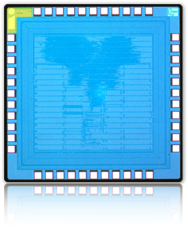
The first silicon implementation of the EnCore processor is a test-chip code-named Calton, fabricated in a generic 130nm CMOS process. All of the EnCore test chips are named after hills in Edinburgh; Calton, being the smallest, is the first of these.
The Calton test-chip contains a baseline configuration of EnCore, together with on-chip Instruction and Data caches, within a system-on-chip (SoC) design that provides external interfaces and control logic for the processor.
CPU Architecture
- 5-stage scalar, fully interlocked instruction pipeline
- Precise exceptions
- Configurable instruction cache
- Configurable data cache
- Up to 32, two level interrupts
- 32 general purpose registers, extendible to 64
Compact 32-Bit RISC ISA
- 16- and 32-bit instructions for high code density
- No overhead for switching between 16- and 32-bit
- Single-cycle instruction execution
- Up to 190 dual, single or zero operand instructions
- Up to 64 directly addressable core registers and 32 conditional execution codes
- Flexible addressing modes
- Optional user-defined instruction-set extensions
Facts and Figures
- 130nm implementation of EnCore processor in baseline configuration extended with barrel shifter, multiplier, and a full set of 32 GPRs.
- Contains bus interface and system control functions, in addition to the processor.
- Implemented with 8KB direct-mapped I-cache and D-cache.
- Complete system-on-chip occupies 1 sq.mm of silicon at 75% utilization.
- Chip-level power consumption is 25 mW at 250 MHz.
- First silicon samples operate above 375 MHz at typical voltage and temperature.


