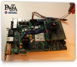
The motherboard is an off-the-shelf Xilinx ML507 board that is programmed to act as the system bridge, providing access to the rest of the system. A made-to-purpose daughter-board is mounted on columns of connectors near the right edge of the board, that also powers the chip. The mictor ribbon across the centre reliably conveys the clocks, bus signals, and the JTAG link to the EnCore chip.

The CPU clock is generated on the motherboard and divided by the Calton chip and then fed back to the FPGA system bridge as the bus clock. The bus divider, or ratio between the CPU clock and bus clock, is adjustable by host side software. For Calton, the FSB can be set to anything from 1/16 of the CPU clock to just the same speed, subject to electrical characteristics of the connection. By leveraging ML705's programmable clock generator, this setup allows us to run the processor with a variety of clock combinations across a spectrum up to 375MHz.
The picture shows the complete testing setup, comprising the FPGA motherboard, a fully assembled daughter-board featuring a big black chip socket, a high-speed mictor connection between the two, and a JTAG link connecting to the host PC. Right above the socket hole the chip is held with tweezers.


