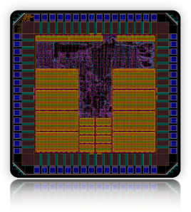
The second silicon implementation of an extended EnCore processor is a test-chip codenamed Castle, fabricated in a generic 90nm CMOS process. All of the EnCore test chips are named after hills in Edinburgh; Castle is named after the rock on which Edinburgh Castle is built.
The Castle chip contains an extended version of the EnCore processor, together with a 32KB 4-way set-associative Instruction Cache, and a 32KB 4-way set-associative Data Cache. It is embedded within a system-on-chip (SoC) design that provides a generic 32-bit memory interface, as well as interrupt, clocks and reset signals.
CPU Architecture
- 5-stage scalar, fully interlocked instruction pipeline
- Precise exceptions
- Configurable instruction cache
- Configurable data cache
- Up to 32, two level interrupts
- 32 general purpose registers, extendible to 64
Compact 32-Bit RISC ISA
- 16- and 32-bit instructions for high code density
- No overhead for switching between 16- and 32-bit
- Single-cycle instruction execution
- Up to 190 dual, single or zero operand instructions
- Up to 64 directly addressable core registers and 32 conditional execution codes
- Flexible addressing modes
- Optional user-defined instruction-set extensions
Reconfigurable Instruction Set Extensions
- Based on the Configurable Flow Accelerator Architecture
- Supports up to 64 reconfigurable extension instructions
- Up to 12 inputs and 8 output values per extension instruction
- 32 extension registers, organized as vectors of length 4
- Up to 4 independent 32x32 multiplications, additions and shifts per extension instruction
- Fully-pipelined over 3 pipeline stages, to allow high speed operation
Facts and Figures
- 90nm implementation is based on a generic free foundry libraries, and a stack of 9 metal layers.
- Complete design occupies 2.25 sq.mm on a 1.875 x 1.875 mm die. This includes the baseline CPU, the reconfigurable CFA extension logic, two 32KB caches, and the off-chip interfaces.
- Designed to operate on a core voltage of 0.9V to 1.1V, with 2.5V LVCMOS I/O signals.
- Packaged in a 68-pin Ceramic LCC.
- First silicon samples operate at 600 MHz.
- Chip-level power consumption is 70mW at 600 MHz, under typical conditions.
- Complete design flow, from RTL to GDSII, was performed by the PASTA team. This was based on an in-house developed design flow using Synopsys Design Compiler for topological synthesis, and IC Compiler for automated place-and-route.
- Over 97% of all flip-flops in the design were automatically clock-gated during logic synthesis.
- LVS and DRC checks were performed using Calibre, from Mentor Graphics.


